How to Avoid Costly PCB Fabrication Mistakes - Essential PCB Layout Design Tips
We have written this blog to help newcomers to PCB design by outlining best practices and avoiding familiar layout and prototype PCB fabrication mistakes. We’ll wrap the article up with some insights into emerging design trends and what we think the future of printed circuit board fabrication may look like in a few short years.
Core PCB layout design principles and best practices
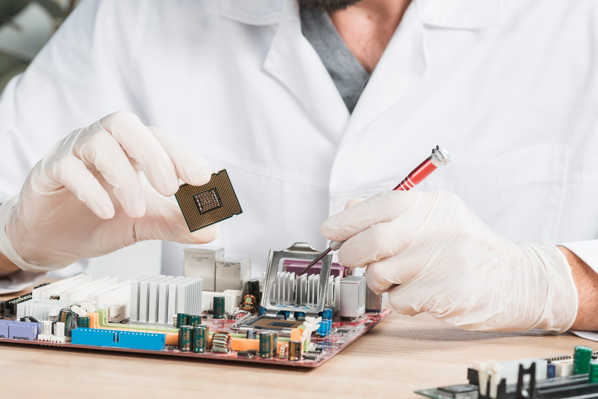
Designing a high-performance, reliable printed circuit board (PCB) requires several key disciplines. Electrical engineering obviously comes into play, with an understanding of components such as resistors, capacitors, and inductors, as well as the fundamentals of power and signal integrity.
Technicians also require knowledge of CAD and PCB layout design. The principles of Component placement significantly affect performance and durability, and a technician can correctly route paths and stack layers of a PCB.
When it comes to printed circuit board fabrication, manufacturing, and assembly, skills are required in materials selection and understanding mechanical fit and tolerances.
The prototype PCB fabrication checklist
PCB layout design is about translating an electrical schematic into a manufacturable, reliable, and testable board. These are the fundamentals every designer should master:
- Define a proper stackup with at least one ground plane.
- Place decoupling caps close to power pins.
- Keep high-speed traces short and use 45° bends.
- Add the appropriate thermal vias.
- Run the fab’s DRC before sending Gerbers.
- Ensure silkscreen does not overlap pads.
- Provide test points for key nets.
Early mistakes that can have significant consequences during production
Seemingly minor oversights during the design and layout phase can later escalate into hugely costly production issues. A mismatched component, an incorrectly calculated tolerance, or a misaligned trace can be picked up during prototype PCB fabrication by your chosen PCB manufacturer before printed circuit board fabrication begins. When you submit your design file, it will be assessed and checked for common mistakes. If you have a good relationship with your PCB manufacturing partner, they may be able to correct errors, suggest more appropriate components, and advise on trace layout.
Here are some of the most common technical PCB design mistakes to avoid at all costs:
- Not giving appropriate consideration to stackup /planning. That can result in a loss of signal integrity and potential re-routing.
- Placing decoupling caps too far from IC pins. Causes power instability and noise.
- Splitting ground planes under high-speed nets can introduce complex EMI issues.
- Not paying attention to fab specs results in unmanufacturable or needlessly expensive boards.
How prototype PCB fabrication is evolving in 2025 and beyond
The pursuit of ever smaller devices that are capable of ever-greater achievements continues at a very rapid pace. Flexible PCBs are now a reality and are entirely practical for use in clothing and worn medical devices. As with all industries, AI is allowing for rapid testing and optimization of components and their placement.
Looking to the future, within five years one can reasonably expect AI to advance significantly to the point where the whole process and design cycle of printed circuit board fabrication and PCB layout design are fully integrated and delivered at an astonishing rate. Design and manufacturing errors will be reduced further, with less waste and newer more eco-friendly materials in widespread use.
If you wish to stay ahead of all the latest innovations in the world of PCB design and manufacture, connect with leading PCB manufacturer Bay Area Circuits.